A group of scientists has developed special photonic chips
Russian scientists have created photonic chips that have surpassed the parameters of photonic integrated circuits from the world's leading companies. The unique technology was developed by the team of the scientific and educational center “Functional micro/nanosystems” — a joint cluster of MSTU. N.E. Bauman and the All-Russian Research Institute of Automation named after. N.L. Dukhova.
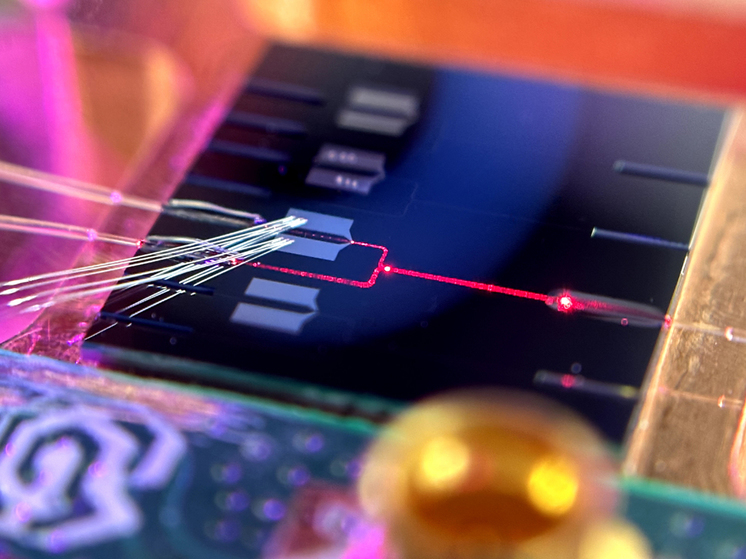 Photon integrated circuit for optical quantum and neuromorphic computing, manufactured at the Research Center for Physics and Mathematics
Integrated circuits, which use light instead of electrical current to transmit data, have been around since the 1990s. The advantage of the photonic chips they use over conventional semiconductor transistors is that information is transmitted not through metal wires, but through waveguides (channels that direct light). This gives new devices an advantage in signal transmission speed, energy saving (light, unlike electric current, experiences no resistance when passing through a waveguide) and protection against hacking (the photonic chip does not store information in memory — all calculations are performed by it simultaneously).
As the Ministry of Education and Science told MK, a team of scientists has developed a unique technology for manufacturing photonic integrated circuits. The minimum size of Russian photonic structures is 50 nanometers (nm), and optical signal loss (a key quality characteristic) in Bauman circuits does not exceed 5 decibels per meter. These figures are several times higher than the results of the world industry leaders.
And what helped Russian scientists get ahead was a new multilayer technology for creating waveguides for photonic integrated circuits. Until now, one of the obstacles to the creation of highly efficient photonic processors has been high signal losses in the optical channels through which photons propagate.
Overcoming this problem by Russian scientists became possible thanks to the technology of creating waveguides from silicon nitride with ultra-low losses. They turned out to be submicron in size, with a surface and edge roughness of no higher than 1 nanometer, which is significantly less than the parameters obtained using traditional technology.
Photon integrated circuits are one of the key elements for creating optical quantum and neuromorphic processors, “sharpened” » to accelerate artificial intelligence systems. That is, as they explained to us at MSTU. Bauman, they are very necessary where parallel calculations are carried out — this is their specificity. It is expected that in the near future photonic integrated circuits will be included in supercomputers along with semiconductor ones. But there is no question of replacing all traditional semiconductor processors with them. For example, processors to provide brain-computer interface technology can operate on standard transistor chips.
According to the rector of MSTU Mikhail Gordin, the new technology can be implemented in cartridges for the latest DNA sequencers, neuromorphic chips for AI, optical quantum processors or lidars for drones.





































Свежие комментарии